eecs270.org
Project 3: Combinational Calculator
| Component | Points |
|---|---|
| Autograder | 75 |
| Lab Signoff | 30 |
| Total | 105 |
Due Date: February 11, 2026 at 11:59 PM
Before Starting
Review two’s complement arithmetic and adders from lecture before starting this project.
Starter Files
Design Specification
The goal of this project is to design CombCalc, a 4-bit two’s complement combinational calculator. It takes a 3-bit opcode OP and two 4-bit operands A and B, and produces a 4-bit result R along with an overflow flag ovf.
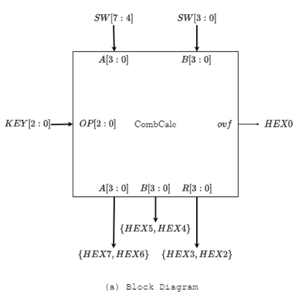
Top-level: Project3 Module
This module connects CombCalc to the FPGA pins.
Top-level Project3 interface:
| Net | Size | Direction | Description |
|---|---|---|---|
SW[7:4] |
4 bits | Input | Operand A |
SW[3:0] |
4 bits | Input | Operand B |
KEY[2:0] |
3 bits | Input | Opcode OP (active low) |
HEX7, HEX6 |
7 bits each | Output | Signed-magnitude display of A |
HEX5, HEX4 |
7 bits each | Output | Signed-magnitude display of B |
HEX1, HEX0 |
7 bits each | Output | Signed-magnitude display of R (or “E” on overflow) |
LEDR[0] |
1 bit | Output | Overflow indicator ovf |
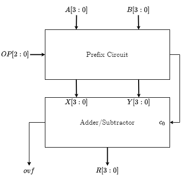
CombCalc Module
The arithmetic core of the calculator.
CombCalc interface:
| Net | Size | Direction | Description |
|---|---|---|---|
A |
4 bits | Input | First two’s complement operand |
B |
4 bits | Input | Second two’s complement operand |
OP |
3 bits | Input | Operation code |
R |
4 bits | Output | Two’s complement result |
ovf |
1 bit | Output | Overflow flag |
Function Table
| OP[2] | OP[1] | OP[0] | R | Operation |
|---|---|---|---|---|
| 1 | 0 | 0 | A + B | A plus B |
| 1 | 1 | 0 | A - B | A minus B |
| 1 | _ | 1 | |B| | abs(B) |
| 0 | 0 | 0 | B + A | B plus A |
| 0 | 1 | 0 | B - A | B minus A |
| 0 | _ | 1 | |A| | abs(A) |
When ovf is 1, the result R is invalid and HEX0 should display “E”.
Arithmetic Core
The computational engine is a parameterized two’s complement Adder/Subtractor. A prefix circuit generates inputs X[3:0], Y[3:0], and c_0 from A, B, and OP so that the Adder/Subtractor output implements the function table above.
Signed-Magnitude Display
Operands A and B as well as the result R must be displayed in signed-magnitude decimal on pairs of 7-segment HEX displays:
- The left HEX of each pair shows the sign: blank for non-negative, or the minus-sign segment (segment 6 on) for negative values.
- The right HEX of each pair shows the absolute value as a decimal digit (0–9).
- On overflow, HEX0 should display the letter “E”.
The HEX displays are active low (0 turns a segment on). Segment numbering and the ten decimal digit renditions are shown below.
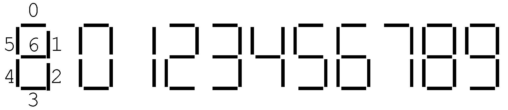
Figure 3: Segment numbering and rendition of the ten decimal digits.
Example: displaying -5
The two’s complement value 4'b1011 = -5 should be displayed as:
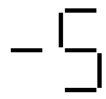
The negative sign is rendered on the left display by turning on only segment 6, and the magnitude 5 is rendered on the right display by turning on all segments except segments 1 and 4:
| Two’s Complement | Sign (Left HEX) | Magnitude (Right HEX) |
|---|---|---|
4'b1011 |
7'b0111111 |
7'b0010010 |
Table 1: Two’s complement encoding for -5 and the corresponding HEX display bits (active low).
Implementing the conversion as a look-up table
The two’s-complement-to-signed-magnitude conversion is best implemented as a look-up table indexed by the 4-bit input (treated as an unsigned index 0–15). Verilog provides syntax for declaring such tables:
reg [6:0] TC4Mag [0:15];

initial begin
    ...
    TC4Mag[11] = 7'b0010010;  // 11 in unsigned = 1011 in binary = -5 in two's complement
    ...
end
The first line declares TC4Mag as a 16-row table where each row is a 7-bit word (the HEX pattern). The initial block populates each row. Row indices must be written in decimal. The bit string 1011 is interpreted as the unsigned index 11 when locating the row, while its two’s complement interpretation is -5.
Design Notes and Hints
- Operator restriction: You may use only basic logical operators (
and,or,xor,not, etc.) and the ternary operator? :. Do not use Verilog’s high-level procedural operators: no+,-, comparisons,if/else, orcasestatements. Those will be introduced in Project 5. - One adder only: You must design a single parameterized Adder/Subtractor module. Do not use Verilog’s
+operator, and do not instantiate more than oneAddSubmodule. - Decompose the design: Split
CombCalcinto (a) the arithmetic core and (b) the signed-magnitude display converters. Design and test each independently. - HEX displays are active low: drive a segment to 0 to turn it on, 1 to turn it off.
- KEYs are active low: a pressed KEY reads as 0.
OPshould reflect which KEYs are pressed. - LabsLand KEY mapping: the LabsLand web interface cannot register multiple simultaneous KEY presses by mouse. Use the keyboard keys
0,1,2,3to activateKEY[0]–KEY[3]. For example, to compute A+B press keys0,1, and2together. - Testbench: Write
TestBench3.vto cover representative opcodes, operand sign combinations, and overflow cases. The autograder grades coverage, so plan your cases deliberately rather than enumerating all 2^11 inputs.
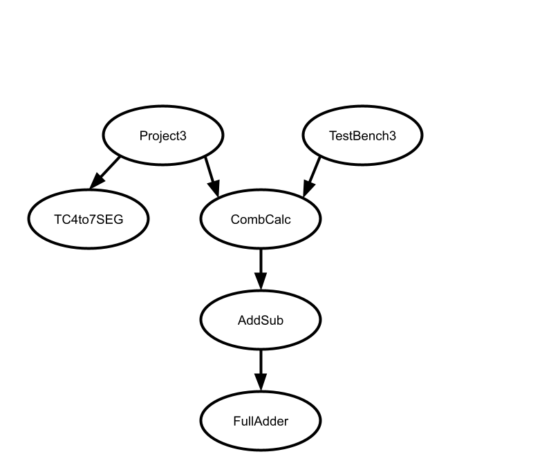
Deliverables
| File Name | Task | Testing Process | Grading Process |
|---|---|---|---|
| CombCalc.v | Implement the arithmetic core | ModelSim | Autograder |
| AddSub.v | Implement the parameterized Adder/Subtractor | ModelSim | Autograder |
| FullAdder.v | Implement the 1-bit full adder | ModelSim | Autograder |
| TC4to7SEG.v | Implement the two’s complement to 7-segment converter | ModelSim | Autograder |
| TestBench3.v | Write test cases for CombCalc | ModelSim | Autograder |
| Project3.v | Connect CombCalc to FPGA inputs and HEX displays | LabsLand | Signoff |
To ensure that your design works with the Autograder, do not modify file names, module names, or interfaces for any of the starter files. All files must be submitted to the Autograder for grading and feedback.
The signoff will be conducted in your assigned lab sections the week after the project deadline.