eecs270.org
Project 4: Timing and Delay
| Component | Points |
|---|---|
| Task 1: Combinational Delay | 16 |
| Task 2: Ring Oscillator Frequency | 24 |
| Total | 40 |
Due Date: February 25, 2026 at 11:59 PM
Before Starting
In this project, you will use ModelSim to analyze the timing behavior of two circuits: a small combinational circuit and an N-stage ring oscillator. You will not design any new circuits; you will measure propagation delays and oscillation frequencies.
Helpful resources:
Starter Files
No starter files are provided. You will create your own ModelSim projects and Verilog files for this lab.
Design Specification
Task 1: Combinational Delay Calculation
Compute the maximum input-to-output propagation delays for the circuit in Figure 1.
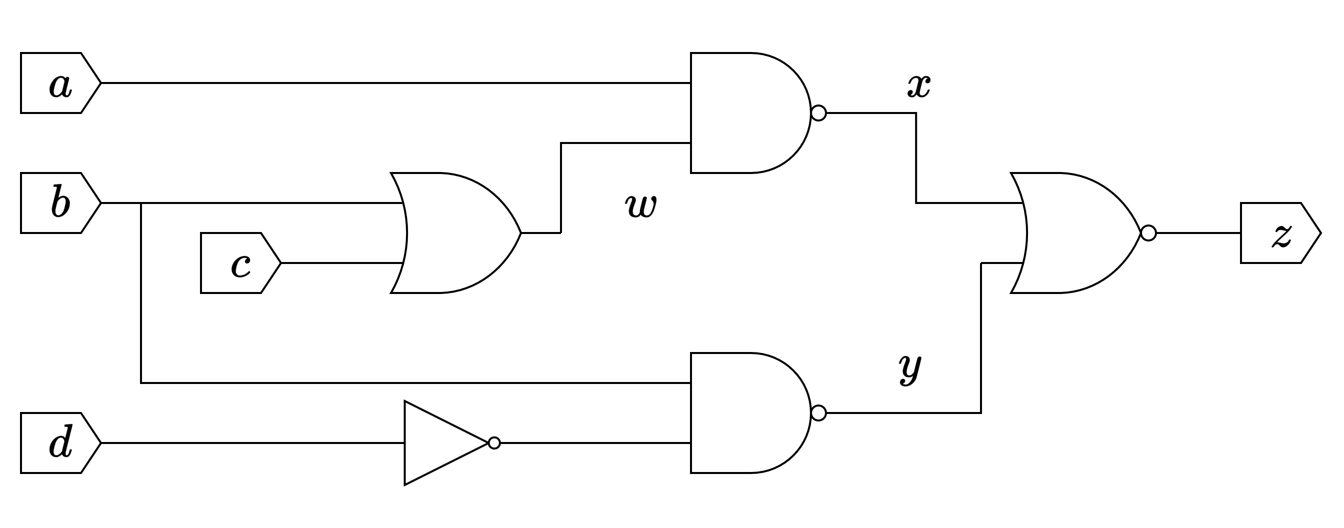
Figure 1: Circuit for combinational timing analysis
Steps:
- Create a ModelSim project for this circuit.
- Toggle each input from 0 to 1 and from 1 to 0 while holding the other inputs at appropriate fixed values.
- Measure the delay between the input transition and the corresponding transition on output z.
Repeat under both scenarios below:
- Unit Delay: tpLH = tpHL = 1 for all gates
- Specified Delay: use the rise and fall delays below
| Gate | tpLH ns | tpHL ns |
|---|---|---|
| nand | 6 | 7 |
| nor | 15 | 10 |
| or | 17 | 12 |
| not | 1 | 2 |
Record your results in the following table format:
Table 1: Combinational path delays for the circuit in Figure 1
| Input i | Unit Delay tpLHi→z | Unit Delay tpHLi→z | Unit Delay max(tpLHi→z, tpHLi→z) | Specified Delay tpLHi→z | Specified Delay tpHLi→z | Specified Delay max(tpLHi→z, tpHLi→z) |
|---|---|---|---|---|---|---|
| a | ||||||
| b | ||||||
| c | ||||||
| d |
Task 2: Ring Oscillator Frequency
Analyze the oscillation behavior of ring oscillators of different sizes. A ring oscillator consists of a NOR gate and N - 1 inverters connected in a ring; when enable transitions from 1 to 0, the circuit begins to oscillate.
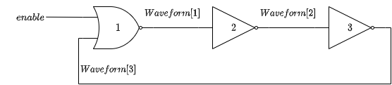
Figure 2: 3-stage ring oscillator
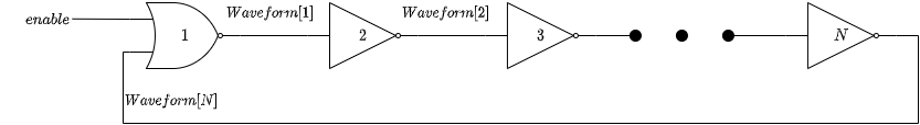
Figure 3: N-stage ring oscillator
The oscillation frequency is f = 1/P, where P is the period measured between corresponding transitions on the same waveform. Use ModelSim’s named cursors to measure P precisely.
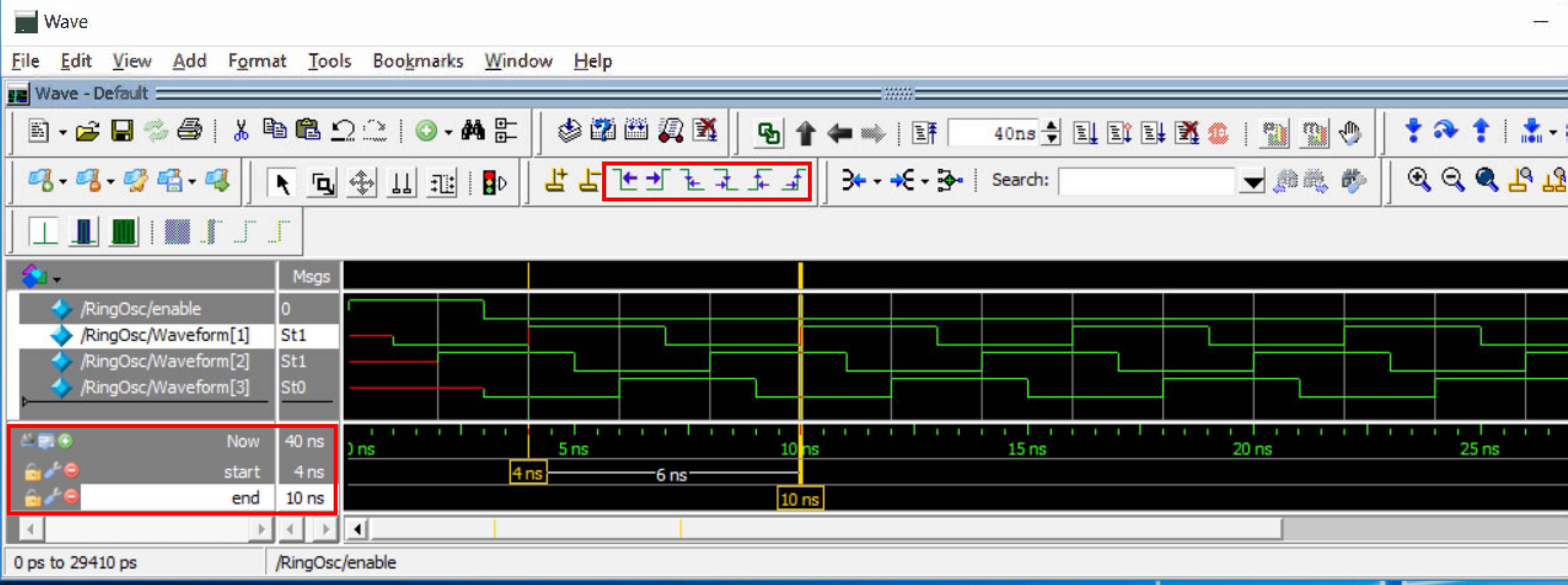
Figure 4: ModelSim waveform for a 3-stage ring oscillator (unit-delay gates)
Use the parameterized Verilog module below as the starting point for your simulation. You must replace initDELAYExpression with an arithmetic expression in terms of N, notDELAY, and norDELAY that is long enough for the waveforms to stabilize before oscillation begins.
// Parameterized Ring Oscillator
`timescale 1ns/1ns

module RingOsc();
    reg enable;             // When 1, stop; when 0, start
    parameter N = 9;        // Number of stages (must be odd)
    parameter notDELAY = 10;
    parameter norDELAY = 15;
    wire [N:1] Waveform;

    genvar i;
    generate
        for (i = 1; i < N; i = i + 1)
            begin : notGates
                not #notDELAY notGate(Waveform[i+1], Waveform[i]);
            end
        nor #norDELAY norGate(Waveform[1], Waveform[N], enable);
    endgenerate

    initial begin
        enable <= 1; #initDELAYExpression;
        enable <= 0;
    end
endmodule
The parameter keyword allows you to easily set a constant value for N and the gate delays without having to rewrite the entire module. This can come in useful for future projects (especially Projects 6 and 7).
This module generates a ring oscillator with N stages from a single NOR gate and N-1 inverters. When enable is 1, the output of the NOR gate is 0, disabling the oscillation. When enable is 1, the NOR gate functions as an inverter and the circuit oscillates. In order to ensure that all gates in the oscillator have value, the initDELAYExpression must be long enough for the constant disabled NOR output to propagate through all N stages.
Steps:
- Create a ModelSim project using the parameterized module above.
- Simulate for
N= 3, 5, 7, 9, 11 - Record period and frequency under both scenarios:
- Unit delay:
notDELAY = norDELAY = 1ns - Specified delay:
notDELAY = 2ns,norDELAY = 4ns
- Unit delay:
Table 2: Period and frequency of oscillation for ring oscillators of different lengths
| N | Unit Delay P (ns) | Unit Delay f (MHz) | Specified Delay P (ns) | Specified Delay f (MHz) |
|---|---|---|---|---|
| 3 | ||||
| 5 | ||||
| 7 | ||||
| 9 | ||||
| 11 |
Design Notes and Hints
- For Task 1, it is possible that a single input transition does not affect the output.
- If you are seeing many
xs in the Task 2 waveforms, theinitDELAYExpressionmay not be long enough. - It may be helpful to calculate the expected delays and frequencies by hand, but you MUST write Verilog and simulate it to earn credit for this project.
Deliverables
Submit a single PDF plus all Verilog files used, to Canvas.
| Item | Task | Format |
|---|---|---|
| Table 1 (completed) | Combinational path delays for Figure 1 | |
| Table 2 (completed) | Ring oscillator period and frequency | |
| Period formulas | P as a function of N for unit delay and specified delay | |
| Verilog sources | All .v files used to produce your results |
Canvas upload |