eecs270.org
Project 5: Up-Down Counter
| Component | Points |
|---|---|
| UpDownCounterV1 Autograder | 50 |
| UpDownCounterV2 Autograder | 50 |
| Total | 100 |
Due Date: March 11, 2026 at 11:59 PM
Before Starting
Review the lectures on sequential design before starting:
- Sequential Verilog Primer
- Sequential Design Examples (slides)
- SequenceDetectorV1.v - style reference for V1 (separate combinational logic +
always @(negedge Clock)block) - SequenceDetectorV2.v - style reference for V2 (single
alwaysblock)
Starter Files
Design Specification
The goal of this project is to design a 2-bit UpDown saturating counter as a synchronous sequential circuit using negative edge-triggered D flip-flops. You will build two versions of the counter to practice different styles of describing sequential behavior in Verilog.
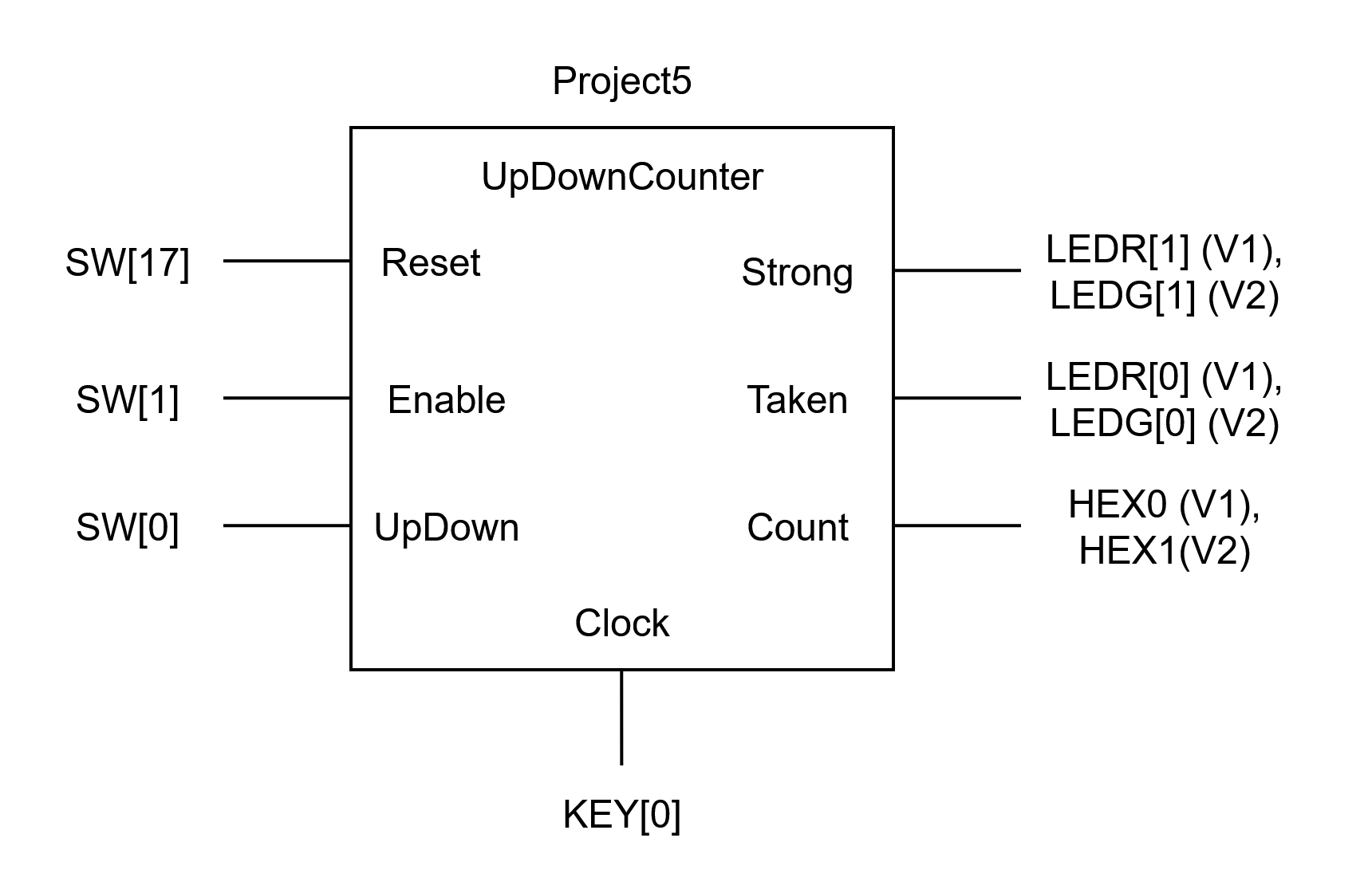
Figure 1: UpDown Counter interface
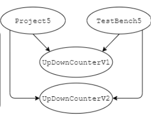
Figure 2: Module instantiation graph
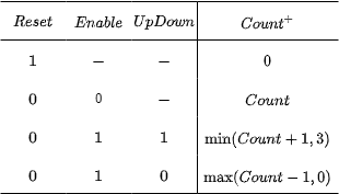
Figure 3: Function Table
Counter behavior:
- The
UpDowninput selects direction:UpDown = 1counts up,UpDown = 0counts down. - The counter saturates: it holds at 3 when counting up and at 0 when counting down.
Outputs:
Taken: asserted when count is either 2, 3.Strong: asserted when count is either 0, 3.Count: current counter value displayed as a decimal digit on a HEX display.
Clock: Use KEY[0] as the clock input. State changes occur on the negative edge of the clock. Keep in mind that KEY[0] is active low, so pressing it creates the falling edge that triggers your flip-flops and releasing it creates the rising edge.
UpDownCounterV1
Implement combinational next-state and output logic using assign statements and the behavioral logic operators (&, |, ^, ~). Flip-flops should be implemented inside an always @(negedge Clock) block, with Reset handled inside the same always block. Use SequenceDetectorV1.v as a style reference.
UpDownCounterV1 interface:
| Net | Size | Direction | Description |
|---|---|---|---|
Clock |
1 bit | Input | Negedge-triggered clock (from KEY[0]) |
Reset |
1 bit | Input | Synchronous reset |
UpDown |
1 bit | Input | 1 = count up, 0 = count down |
Taken |
1 bit | Output | High when count is 2 or 3 |
Strong |
1 bit | Output | High when count is 0 or 3 |
Count |
7 bits | Output | 7-segment encoding of current count (0-3) |
UpDownCounterV2
Implement the counter in the style of SequenceDetectorV2.v. You may NOT use an adder or the + operator in this version.
UpDownCounterV2 interface:
| Net | Size | Direction | Description |
|---|---|---|---|
Clock |
1 bit | Input | Negedge-triggered clock (from KEY[0]) |
Reset |
1 bit | Input | Synchronous reset |
UpDown |
1 bit | Input | 1 = count up, 0 = count down |
Taken |
1 bit | Output | High when count is 2 or 3 |
Strong |
1 bit | Output | High when count is 0 or 3 |
Count |
7 bits | Output | 7-segment encoding of current count (0-3) |
Top-level: Project5 Module
Project5 and TestBench5 both instantiate both versions of the counter and wire them to the board as shown in Figure 1.
Top-level Project5 interface:
| Net | Direction | Physical Description | Correspondence |
|---|---|---|---|
SW[0] |
input | rightmost switch | UpDown (both versions) |
KEY[0] |
input | rightmost pushbutton | Clock (both versions) |
KEY[3] |
input | leftmost pushbutton | Reset (both versions) |
LEDR[1:0] |
output | red LEDs | {Strong, Taken} for V1 |
HEX0[6:0] |
output | 7-segment display | Count for V1 |
LEDG[1:0] |
output | green LEDs | {Strong, Taken} for V2 |
HEX1[6:0] |
output | 7-segment display | Count for V2 |
Design Notes and Hints
KEY[0]is active low, so pressing it creates the falling edge that triggers your flip-flops.- The HEX displays are active low - drive a segment to 0 to turn it on.
Countis output as a 7-segment encoding, not as a raw 2-bit number; build the decoder as part of your counter output logic.- For V2, think about how to express “+1” and “-1” using only gates/muxes on 2-bit values - the saturation condition can simplify this.
- Simulate both versions in ModelSim with
TestBench5.vto debug.
Deliverables
| File Name | Task | Testing Process | Grading Process |
|---|---|---|---|
| UpDownCounterV1.v | Implement V1 using assign + always @(negedge Clock) |
ModelSim | Autograder |
| UpDownCounterV2.v | Implement V2 in SequenceDetectorV2 style (no adder) | ModelSim | Autograder |
| TestBench5.v | Test cases for both counter versions | ModelSim | Autograder |
| Project5.v | Connect both counters to FPGA I/O | LabsLand | Autograder |
To ensure that your design works with the Autograder, do not modify file names, module names, or interfaces for any of the starter files.